Small Audio Power Amplifier Using Op-Amp and Two Transistors
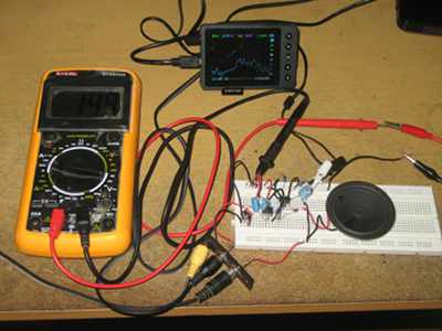
Figure 1. Assembled Small Power Amplifier Using Op-Amp and Transistors
Sometimes we need small power amplifier circuit while we have unused op-amp section in one of our applied chip. Instead of adding more IC (such as LM386 or similar devices), adding two small transistor and several passive components can be cheaper solution if we can employ the unused op-amp section. Using two small transistors (2N3904 and 2N3906), we can build small power amplifier which deliver several hundreds milliwats. The basic circuit is a totem pole transistor pair with small biasing circuit configuration to give small leakage idle-current. Let’s see the schematic diagram of the circuit in the Figure 2. TR1 transistor will be biased by base-emitter voltage, and TR2 by emitter-base voltage, and this series configuration make both transistor are biased by base-to-base voltage. When this base-to-base voltage is lower than two base-emitter forward bias voltages then both transistors will be turned off.
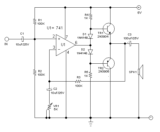
Figure 2. Schematic Diagram of Small Audio Power Amplifier Circuit Using Op-Amp and Two Transistors
Let’s imagine the op-amp is omitted, then the base-to-base voltage is the voltage between R4 and R5 which is dropped by two diodes D1-D2. This voltage is slightly higher than base-to-base bias requirement to produce small leakage current when there is no signal. The op-amp output is connected to the center of diode-resistor biasing circuitry, and this signal manipulate the biasing point. At idle condition, when there is no signal in the input, the output should be bet at Vcc/2. When the signal goes positive, the op-amp output will drive the biasing point to positive side the lower transistor will be switched off and the upper transistor will be driven to give correct voltage at the feedback point pin 3 (the inverting input). The feedback mechanism will set the proper bias current to maintain the voltage level at inverting input (pin 3) to be same with the level at the non-inverting input (pin 2).
Components Selection
Almost any type of op-amp capable of delivering 1-5 mA current can be used for this circuit. Most of any small transistors with maximum collector current handling around 100-200 mA can be used.
- The resistors R1 and R2 should be selected to supply the biasing point at 0.5Vcc, chose as high as possible but keep below 1/10 of op-amp’s input impedance.
- R3 resistor serves as the DC feedback, making sure that the DC level of the output will be same as non-inverting input (pin 2). Choose this resistor as high as possible but keep it lower than 1/10 of op-amp’s input impedance.
- VR1 is provided to set the signal gain, choose any values to get the desired gain adjustment range, and the gain will be (1+(R3/VR1)).
- Capacitor C1 serve as DC decoupler and AC coupler. The simplest rule for DC decoupler capacitor selection is that maximum reactance of the capacitor at the lowest frequency is 1/10 of the input impedance (which is the combination of R1 in parallel with R2).
- Capacitor C1 also serve as DC decoupler and AC coupler. The simplest rule for DC decoupler capacitor selection is that maximum reactance of the capacitor at the lowest frequency is 1/10 of the input impedance (which is the combination of VR1 in parallel with R3).
- Resistor R4 and R5 is similar, and the value can be easily chosen based on the maximum current handling of the transistor. Let say the maximum collector current of the transistors is 200 mA and the current gain is 100, and at maximum condition the output of op-amp is tied to Vcc or Ground (just as a simple approximation, not many types of op-amp can fully swing like this), then we can compute the needed base current is 2 mA. The highet resistance for this resistor is then the supply voltage divided by this base current. 6V/2mA = 3k ohm. We can lower this resistor as low as possible since the feedback mechanism and the dropping diodes makes the circuits always get proper operation, but we have to keep the biasing current of the nonactive transistor to be safely sinked or sourced by the op-mp. Lowering the resistor, although its current can still be handled by the op-amp) to some point also making the dropped voltage (by the diodes) getting higher and it means a higher idle current. We might need to insert series resistor (about 0.5 ohm) on the emitter on each transistor if we want to lower the R4/R5 resistor to maximize the output power.
- Capacitor C3 serve as DC decoupler and AC coupler as well. The simplest rule for DC decoupler capacitor selection is that maximum reactance of the capacitor at the lowest frequency is 1/10 of the series impedance (which is the impedance of the speaker). For small audio power amplifier application, its okay to limit the bandwidth not going to low so the capacitor will be small and cheap.
The Amplifier in Action
See how this small audio power amplifier circuit works when powered and fed with music signal in our Youtube channel below:
What’s the output of this amplifier and how to increase it to 10 watts ?
How to calculate the values of components to get a particular watts output ?