Adjustable Frequency Flip-Flop Circuit Using Inverter Gate
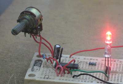
Figure 1. Assembled Inverter Flip-Flop Circuit
This flip-flop circuit uses one potentiometer and one capacitor as the frequency determining components. The assembled circuit is shown in the Figure 1, and the schematic diagram of the circuit is shown in the Figure 2. The circuit consists of one integrated circuit of inverter gates (4069 CMOS or 74C04), one electrolytic capacitor, two resistors, two LEDs, and one potentiometer.
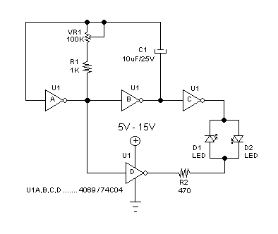
Figure 2. Schematic Diagram of Inverter Flip-Flop Circuit
To analyze how this circuit works, let’s assume an initial condition of U1A output = high, U1B output = low. Let’s label this condition as state 1, where therefore U1C = high and U1D = low. At this state, LED D2 is on and LED D1 is off. The other state, state 2, is where all gates are in the opposite condition, so LED D2 is off and LED D1 is on.
Let’s assume C1 capacitor’s charge is empty at the initial condition state 1 (when first powered). Since U1A = high and U1B = low, then the capacitor C1 will be charged from U1A ouput to U1B output trhough R1 and VR1. At this state the capacitor voltage will rise from zero towards the high level voltage. The voltage of this C1 capacitor is sensed by the U1A input, and once the voltage reach the activation voltage of U1A gate then its output will flip and invert all gate’s states, switching the state from state 1 to state 2.
Right just before the switching of state 1 to state 2, the input of U1A is at the activation voltage level which might be set (by the inverter gate IC design) around half of supply voltage. Right just after the state switching to state 2, this input level is immediately pushed (through capacitor C1) to the high level by the output of U1B which just switched to high. This level is gradually falling down as the capacitor discharge from U1B output to U1A output through R1 and VR1, maintaining state 2 condition before it reach the deactivation level of U1A gate. Once the deactivation level is reach then the state will be back to state 1. See the circuit works in the Youtube video below.
your circuit is good, but i’m sorry i’m still newbie. can you explain what pin in U1 A, U1 B, U1 C, and U1 D? Thank for you answer 🙂