DIY Reverb Pedal Circuit: Spring-Hall Reverb with PT2399 IC
Introduction to Reverberation
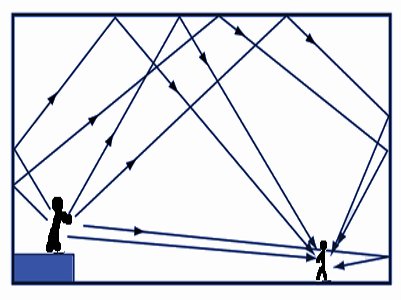
Before getting into the design of DIY reverb pedal circuit, lets see the concept of reverberation first. Real reverberation happens in a performance chamber when the walls and every object inside reflects the sound back and forth. As the sound bounces back and forth in three dimensional space, the reflections creates more and more complex pattern. The natural process shown in the Figure 1 is the illustration of reverberation. In the old days, the only way to reproduce a reverberation effect is by using a real reverberation chamber.
For good effect, someone should build a large room with complex geometry with carefully selected wall material. After that, he should place some loudspeakers at certain location and place a microphone at another location inside the chamber. The first attempt to mimic a room reverberation without a real reverberation chamber is done by a spring reverb tank (see reference [1]). Figure 2. shows the basic construction of spring reverb tank.
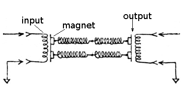
The audio signal drives an input coil that vibrate the spring at one end. The created vibration is then travels to the other end and bounce back and forth between two ends. During it’s travel, the amplitude is decreasing until deceasing. Because of the different traveling speed of high and low frequency waves, the reflection produces more complex waves. In addition, the spring joints adds more complex reflections in the middle of its traveling path. Moreover, different springs arrangement with different characteristics would produce rich and unique resonant characteristics. Finally, a pickup coil picks the reverberated sound at the other end of the spring. The pick-up then returns the signal to the amplifier or the processing circuits.
Digital Modelling of Reverb Effect
Many expert has researched reverberation effect processing in digital domain, and (in my opinion) can be classified on several mainstream methods. Firstly, system response reproduction: this method treat the modeled system as a black-box. However, we don’t care about what happen inside this box. All we need to do is just measuring the output response after we apply an impulse input. After getting the response pattern, a digital processor compute the convolution of the pattern and the input. and use it to modify the signal by convolution processing (see reference [2]). Whether the modeled system is a real concert hall or a real spring, it will just work. It would be very simple to implement but the convolution processing would require very high processing power to run.
Secondly, physical modelling: this method analyze the physical process of the modeled system simulate every physical process in the computation. This produces very realistic realistic sound but the computational cost could be high. However, it depends on the optimization or mathematical simplification of the model. For example, you can see one example of spring reverb modelling at reference [3].
Lastly, synthetic modelling: this model construct a computation model that produce a (perceived) similar effect on the audio output. As long as the perceived result is similar, the computation model might not be related with the physical model. Sometimes I see such model is just an oversimplified model of the physical. Similarly, approximation of the system response by trial and error computation experiment might produce such effect as well. For example, a Schroeder reverb [see ref [4]), can be adjusted to mimic the medium-size hall reverberation by setting up some parameter to certain values.
Electronic Circuit Implementation of DIY Reverb Pedal Circuit: Delay Line Network and Tuned Analog Resonators?
After we analyze that the reverberation phenomenon as the complex echo pattern, we know the principle is simple. Therefore, we can intuitively build such reverb effect circuit using some delay line networks. On the other hand, if we analyze the reverberation phenomenon as a continuous resonance, we might think differently. Therefore, we can think that multiple parallel analog resonators (with different frequency tuning) could generate such effect.
I have been thinking of this analog resonators for years since I learned electronics. It is well known on the oscillator subject, where many of oscillator designs are basically an unstable resonator. Please let me know if there is already analog reverb circuit design which is based on analog resonators. Please write a comment if you find it, so I won’t be reinventing the wheel someday. For the moment, let’s focus on the delay line circuit solution. We will use it for the reverb circuit design, since it has been proven in such applications.
PT2399 Digital Delay Line IC Chip, Low Cost Solution for DIY Reverb Pedal Project
In the old days, the bucket-brigade device is very popular. It uses switched capacitors array to store audio samples in analog voltage is for implementing a delay line function. With the advanced CMOS technology, PT2399 IC from Princeton technology is getting popular. Because of its low cost, it replaces almost all BBD chips. Figure 3. shows the block diagram of the internal circuitry of PT2399 IC chip.
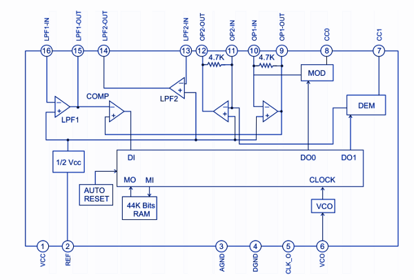
This digital delay line chip is available in 16-pin DIP package, so it will be easy to be handled. Certainly it would be the preferred option for do-it-yourself projects. The minimum delay length is 30 ms and the maximum is 340 ms. This delay setting is easily adjustable by selecting a proper value of an external resistor.
DIY Reverb Pedal Circuit for Simulating Spring and Room/Hall Reverb
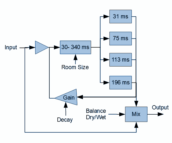
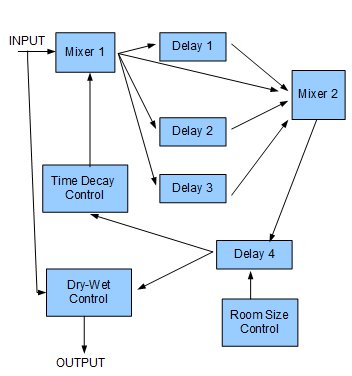
I have created very simple reverb circuit that can simulate spring and room reverb effect. It use 5 delay line integrated circuit chips, and the block diagram is shown in the Figure 4. It has decay time control, room size control, and dry/wet balance control. When we set the room size to minimum, it would sound similar to spring reverb. On the other hand, when we adjust it to maximum then it would produce hall or even cathedral-like reverb.
Reconfiguring The Delay Blocks Structure
If we take a look at Figure 4, we can see that the first delay block can’t be set to 0 second delay since the minimum delay for the PT2399 chip is about 30 ms. The result is that the total shortest delay is 61 ms, and this is not good for simulating soundwave wave propagation inside a spring. By reconfiguring the delay blocks as shown in the Figure 5, we can achieve the shortest delay about 30 ms while minimizing the component count by using only 4 delay chips.
The Complete Circuit’s Schematic Diagram
A testing in digital domain (using Deepstomp platform) has shown that the basic block diagram of the circuit works fine. For the actual hardware, here is the schematic diagram of the reverb pedal circuit (Figure 6). It has four controls: decay time, room size, dry/wet balance, and the output level.
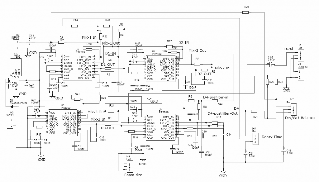
You can see in some component values are missing, and that’s because the final circuit is still under development. We will update with the final value right in this page when the circuit has been successfully tested. You can see that the missing values are primarily on the mixer and filter parts, but you can figure it out from the gain, amplitude range, and the frequency response assumptions to try some values if you want to experiment yourself for finding the best component values.
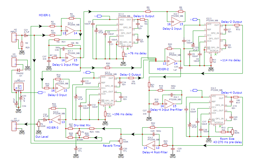
Update (07/13/2020): Restructuring The Schematic Diagram and Adding Some Improvement
The schematic diagram shown in the Figure 6 is hard to read, making it hard to validate and analyze. Now I have redrawn the schematic with some fixes and additional features, see it in the Figure 7. The part list in shown in the Table 1.
| ID | Name | Designator | Quantity |
| 1 | 1N4002 | D1 | 1 |
| 2 | 4k | R1 | 1 |
| 3 | 100k | R2,R3,R4,R25,R26,R27,R28 | 7 |
| 4 | 10k | R5,R8,R10,R16,R20,R30,R9, R6,R7,R14,R15,R17,R18,R19,R23 | 15 |
| 5 | PT2399_MB | IC1,IC2,IC3,IC4 | 4 |
| 6 | 7k2 | R11 | 1 |
| 7 | 14k3 | R12 | 1 |
| 8 | 1k2 | R13 | 1 |
| 9 | 15k | R22,R21,R31 | 3 |
| 10 | 270k | R24 | 1 |
| 11 | 1M | R29 | 1 |
| 12 | LM7805CT | U1 | 1 |
| 13 | 100nF | C1,C2,C5,C6,C9,C10,C11,C12,C15,C16,C17,C18 | 12 |
| 14 | 82n | C3,C4,C7,C8,C13,C14,C19,C20 | 8 |
| 15 | 560p | C26,C28,C36 | 3 |
| 16 | 3n9 | C27,C37 | 2 |
| 17 | 3n3 | C29 | 1 |
| 18 | 1uF | C35 | 1 |
| 19 | A50K | P1,P4 | 2 |
| 20 | B100k | P2 | 1 |
| 21 | B20k | P3 | 1 |
| 22 | IN Header | H2 | 1 |
| 23 | Out Header | H1 | 1 |
| 24 | DC9V Header | H3 | 1 |
| 25 | 4.7uF | C21,C32 | 2 |
| 26 | 47uF | C22,C23,C24,C25,C33,C34,C31,C30 | 8 |
The schematic diagram is now added with signal flow marking for easier analysis. The circuit is optimized for the lowest component count. Here some points which are probably speculative and need more testing and experiment:
- There is no documentation on the op-amp’s open-loop gain and input impedance spec specs of the free op amp section (pin 13-14). I just use 100k resistor for setting up gain and mixing impedance resistors at IC1_2, while example circuit in the datasheet uses about 10-15k resistors. By using 100k resistor, the input impedance of this PT2399 reverb circuit is around 50k, determined by the R3 in parallel with R26-R28 series. The use of high resistance for this circuitry is to avoid external op-amp addition, so the components cunt would be minimal.
- To avoid many dc decoupling capacitors, most internal connections between IC uses DC coupling (only after MIXER-2 has a decoupling capacitor). This may lead to offset error since each IC has it’s own internal references which might have some differences from chip to chip. It is assumed that the difference is small enough and got no much amplification since most of amplifier stages is set around unity gain.
- To avoid redundant filters for input sections of the PT2399 delay lines, all the delay lines uses the filtered signal tapped from Delay-1 input filters output. It is assumed that the output connection in this point is not affected by the loading effect of the internal delay line connection inside the IC-1 chip.
- To avoid the redundancy of the output filter, the filtering of the Delay-1, Delay-2, and Delay-2 outputs is done after mixing. This after-mix filtering is done by Delay-4 input pre-filter.
That’s all what I can say about the progress, and be warned that his circuit is not yet tested. I will publish the result when I have tested it myself, but after understanding some of the assumption I think you can try it yourself to test the circuit and discuss the result here. Any comment are welcome!
References
- L. Hammond, “Electical Musical Instrument,” U.S. Patent 2,230,836, Feb. 2, 1941.
- Fons Adriaensen, “Acoustical Impulse Response Measurement with ALIKI”, 4th International Linux Audio Conference: LAC2006, http://lac.zkm.de/2006/papers/lac2006_fons_adriaensen_01.pdf
- Stefan Bilbao and Julian Parker, “A Virtual Model of Spring Reverberation “, IEEE Transactions on Audio, Speech, and Language Processing, Vol. 18, No.4, May 2010 p.799,https://www.era.lib.ed.ac.uk/bitstream/handle/1842/3718/BilbaoS_A%20Virtual%20model.pdf
- M. R. Schroeder (Bell Telephone Laboratories, Incorporated, Murray Hill, New Jersey),
“Natural Sounding Artificial Reverberation”, Journal of The Audio Engineering Society, July 1962
Great work.
Did you ever get to building and testing this?
Do you have any updates on your progress?
Actually I have designed the PCB and fabricate 10 pcs of the PCBs since 6 month ago, but never get a free time to assemble and test it. I can sent the PCB if you want to test it or do you want the gerber file to produce the PCB and test yourself?
Hey! I’d definitely be interested in some gerbers to test this if you would like me to!
Thanks for trying to help but for now lets wait for testing reports by our builder fellows.. Once all the circuit’s functions pass the test then you can easily design your own PCB version.
Previously I offered the gerber file for the previous commenter because there’s no one that help me testing it. Now several builders have taken my fabricated PCB to test it so we can just wait for their reports.
Are there any more of the PCBs available? I would be up for buying one and testing it out with the other fellow builders.
Unfortunately no, all spare PCBs have been sent to our fellow builders to test.
hey I am a technician and i want to try this project so can you give me the pcb or gervber file plss…..
I’d like to try my hand at building a few of these. Would you mind sharing the Gerber files? Sure I’ll wait to see how the testing goes before ordering boards, (always wise with a mixed signal circuit). But if it works out and Imake a dozen I’ll be glad to share a few too.
No, the gerber file is far from perfect.. many pads and tracks are too small and need many editing to be a good design. Let’s see if the circuit got validated first and I’ll fix the PCB design then.
Hi,Mr.Hamuro could you please share the PCB layout. I am beginner electric guitarist and CS student, I am trying to make a pedalboard for the cheapest price possible and after looking for reverb circuits all over the internet, your design seems the most intriguing because most DIY reverb pedal use 1-2 PT2399(didn’t sound that great) or Belton Brick(Sound’s the best but expensive ).And after searching around about the Belton,I found that it uses 3 PT2399.So your design could possibly be even better and cheaper to make. I would love to try the circuit out and place it on my pedalboard and possible give you a clean + reverb track to post here.
Hamuro,
What has become of this circuit? I did some research and found quite a few of this style of design for sale all over Amazon. one in particular that is very much like yours is from a guy called Azor music. wondering if you took this to market.
I am an engineer and hobbyist amp and effects builder. I built a amp with a true spring reverb circuit from a Fender deluxe. but its noisy, so i pulled it out and am trying to use a stomp box reverb unit I bought on line. it works but is very fake sounding reverb. Would like more control over how the room effect works. really want to integrate this circuit into my amp. have you taken this further?
Hi David, I don’t have any plan to make a commercial product of this circuit so far. This circuit hasn’t been tested yet. You can build this circuit to test yourself, and you can report the result here so I can guide you to make some fix or improvement if needed.
Hi Hamuro,
I am watching this idea with great interest – if you have any further files or ideas to share I would be very grateful. I know you said you weren’t happy with the gerbers but I would love to see your layout. I’d like to make this and give you feedback
I noticed in the BoM that there appears to be two lines of 10k resistors – one with 10k and one with 10K. Is this a simple typo and they are meant to be together, or are they meant to be different values?
Thanks for making this circuit and idea public!!! Very cool project
Ah yes that’s a typo, thanks for you report, I have corrected it.
After seeing your circuit, and after a few of my own experiments with this chip on chorus and delay effects, I have decided to take this idea a step or two further…
I love the idea of using multiple chips in parallel to implement a decent reverb – this is a fantastic concept. But I also love the various uses of this chip for chorus, flange, delays, vibrato etc…
I currently do a lot of work with microcontrollers and have a few digital resistor chips hanging around, so I have now got an MT8808 analog 8×8 grid on order. I am going to build 4-5 modules just like you have but make the delay of each one digitally controlled (possibly through pin2 like the Little Angel chorus), and multiplex their inputs and outputs to several busses so that they can be rewired in different ways.
This will let me implement your circuit programmatically, and then play with different reverb times, but will also allow me to join the units in serial to get long clean delays, use all sort of modulation on the delay to get chorus and flanging effects, etc., even wire two together to get a P Chorus effect
This should be fun!
What a nice idea! Have fun!
There is still a discrepancy. On the BOM, R27 and R28 have the values at 100K. On the schematic, R27 and R28 have their values at 10K. I used the BOM to set the values in a Kicad schematic and since R25 and R26 also have their values at 100K on both, I used 100K for all four around the Wet/Dry Mix. I haven’t built this yet and since I’m cutting the board at home on a CNC I’ll populate the board as such unless I see something different here.
Sorry about the schematic error, you are right, R27 and R28 should be 100K.
I tried building this via breadboard. It did work! And i can say it is verified! But my only problem is it’s really really noisy and there’s huge pop on my on/off toggle switch even though i tried installing input anti-pop drop down resistors (2.2M). Reverb time and room size knobs are problematic as well. They squeal when knob at full and and i encounter infinite feedback every time they’re on full. I’ve used the exact layout and component values as the schematics here. This is a good sounding reverb pedal except for those problems.
Thank for your report, we will update the schematic when we find the fix.
I am a retired electronics engineer. I have tried with simple 2 x PT2399 and it worked fine. But no control over delay and room size. I would like to try with your design. Can you share your pcb design. M k das
Before further troubleshooting, please make sure that your on/off switch is a standard bypass wiring, not the power supply on/off switch (it should be always on).
The DC level of input and output points (H1 and H2) is already zero and produce no click/pop when connected/disconnected to other signal point with zero DC level. Make sure C21 and C32 are installed with correct polarity to zero the in/out DC levels.
I can confirm it is verified but please hope the author can help us out get rid of the noise. Im already using a good quality isolated regulated power supply
https://selftaughtcreativity.wordpress.com/2021/09/07/new-guitar-bass-diy-pedals-series-vol-5-hamuro-reverb-unverified/
I’ve tried to layout this BRILLIANT design, if you find some error tracking the diagram let me know!! I’m gonna etch this PCB on the next weekend, but if somebody has any complaint just … say it and help me out! (copper side is for a laser printer, if you are planning on doing it tonner-transfer you shoud use simmetry before. Layout by Leoben Conoy. Cheers:!!! And… THANKS MR HAMURO for sharing this great design!!
Great! You made a nice compact layot, I love it!
Your design just seemed the greatest alternative to BELTON BRICKS and I’ve learn a lot too about block diagrams used to have a most understandable design. BRILLIANT, SUPERB!!! I’ve updated it again today just correcting a little fail in values etc, and adding a little bridge, but this last desing is the last I hope after debbuging it again. This weekend (or maybe tonight) I’ll try to make it in the laser and have at least a PCB to start soldering. ThankS!!!
Although my reverb uses more delay lines, the dispersion of the bouncing pattern maybe not as good as the Belton brick because the lack of modulation. To improve it, we can add a bit of low frequency modulation to the first delay line, maybe in the range of 0.5 – 2.0 Hz. I don’t implement that modulation in the current design for the shake of simplicity.
That low frequency modulation improve sounds really promising 🙂 Not very sure about where that mod could be connected, maybe pin 6 or pin 2 input? Sadly I’ve get lost with modding stuff like this… I’m not very familiar with this PT2399 chip, just some delays and choruses done but keeping track on existing schematics :/ If you can give advice about the mod I’ll be glad making a prototype with it to taste your ideas. And thanks for answering too! Very kind of yours!! Cheers have a good day!! (my email adress is afectual@hotmail.com if you would like to exchange emails or need some layout development in the future)
To modulate the room size delay line, If you have a sine wave output with around 5V amplitude, then you can inject to pin 6 through a series of 220k resistor and 1uF nonpolar capacitor.
http://www.learningaboutelectronics.com/Articles/Sine-wave-generator-circuit-with-a-555-timer.php
I was thinking maybe something like this? WIEN BRIDGE OSCILLATOR ?
Maybe you can enlight me as I’m just an electronic hobby enthusiast, but not very good at mathematics xD
https://selftaughtcreativity.wordpress.com/2021/09/12/691/
I’ve made up these, not very elegant… but I think will work with the circuit’s ‘idea’. My ‘sine’ output through a series of a 220k and a 1uF (non polar) would do the trick? I should taste it and update layout (some extra space left 😉 ). I’ll let you know what happens! ^^ I’ll keep in touch!
Not a perfect sine but give it a try and see how it affects the sound
It fits in a 1590B if you were asking yourselfs 😉
Hello guys!Would it be possible to have the gerber files?I really want to try this thing!!!!!!Thanks you so much!!!
in 2009 I made a circuit using 4 PT2399s in parallel with individual time and level adjustments to generate random reverb and could be switched to use in series also generating an echo of more than 2s
Hola, he contruido este circuito pero encontré algunos inconvenientes, por ejemplo el potenciometro Decay Time apenas puede ajustarse ya que se realimenta quedando en un bucle, otro problema es el fuerte zumbido del clock que se vuelve intolerable. Revisé el circuito varias veces y es tal cual. Mejoró cambiando el potenciometro Decay Time por uno de 20k, pero no mucho.
Hello, I have built this circuit but I found some drawbacks, for example the Decay Time potentiometer can hardly be adjusted as it feeds back into a loop, another problem is the loud hum of the clock that becomes intolerable. I’ve checked the circuit several times and it’s just as it is. He improved by changing the Decay Time potentiometer to a 20k one, but not much.
Hello. I think the block diagram has a problem. If Gain=0, the input signal passes through the delay blocks and reaches the mix block. With this there would be a burst of 4 echoes with no decay and then nothing. In fact, I have implemented that diagram with a microcontroller and it has that problem.