ESP32 I2S-PDM Interface for Digital Guitar Pedal Application
The PDM (pulse-density modulation) has been widely used in the current technology of audio signal conversion (from analog to digital) because its simplicity while achieving high quality conversion. This technology is widely used in digital microphone, and it is basically a sigma delta modulator circuit which is used in many modern audio codec chip as well. It is an interesting feature that ESP32 micro controller has PDM operation mode in its I2S peripheral interface, so it can be a very cheap method to interface with audio input-output, and here I have designed such circuit for digital guitar effect pedal application. Here is the schematic diagram of the circuit:
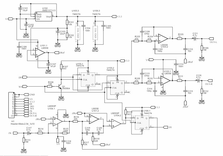
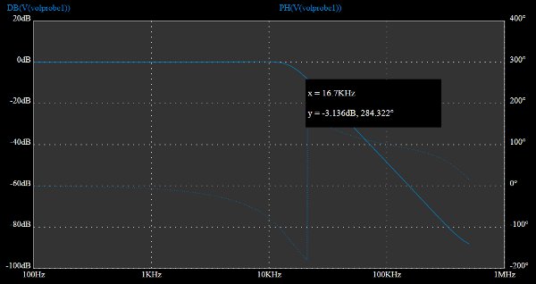
There are two main parts of the circuit: the PDM demodulator and the PDM modulator. The demodulator works by demultiplexing the left and right channel signal data. The WS (word select) input is a clock signal that trigger the D flip-flop (U105.1 and U105.2) to capture the data from the DO input. By using the Q1 transitor to invert the clock, now the first flip-flop (U105.1) will capture the data at the falling edge of the clock signal to get the left signal data. Similar with the first flip-flop, but without inversion, the second one will capture the right data on the rising edge of the clock signal. To recover the analog audio signal, the left and right data is then simply filtered by low-pass filters (U103.2 and U103.1). The filters are third order, with the corner frequency (where the output is attenuated by 3dB) is set at around 16kHz. The frequency response of the filter is shown in the Figure 2.
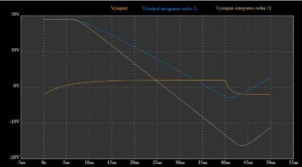
The second main part, the PDM modulator, consist of delta integrator U101.2, the comparator U104.2, and data latch D flip-flop U106.1. The delta integrator is a dual-slope integrator, or order 2 integrator. A dual slope integrator is constructed by adding R118 and C120 into a single integrator (where the output of the op=amp is just connected directly to the C119). The Figure 3 shows the improvement made by the second order (dual slope) integrator compared with a single slope (1st order) integrator.
Circuit Testing Result
The first test for the circuit in the Figure 1 is done partially for the demultiplexing part (Q1, U105.1, U105.2), and the filter (U103.1, U103.2) is simplified by using only one stage RC filter for each channel. For this test, a 1 kHz triangle wave is generated by a software to beep on left and right channel alternatively. The result show that the sound is noisy and presented on one channel only. The inverted clock signal is always low, while the clock input is measured at about 6.15 Mhz. The conclusion is that the transistor inverter is too slow. Here some modification steps that I’ve done and the result:
- I have modified the transistor inverter gate into baker clamp circuit for faster response, but didn’t work
- I have modified the gate to use 74HC14, then it worked on both channel, but the channel was not separated and still noisy.
- I add a termination resistor 330 for clock input (close to the 74HC14) it worked like a charm, the sound (software generated) is clean and the channel separation was perfect. Termination resistor should be placed between input line and 3.3V supply, adding it between clock line and ground didn’t work.
After fixing the demultiplexer part and proving that the output part perfectly works, then the modulator part was tested by routing the input reading to the output. The result is very bad, highly distorted sound only on hard strumming, and completely silent at normal strumming. Here some of the details:
- The data output at Q and -Q is around 70kHz, that’s very bad while the clock is at 6MHz.
- Changing the capacitor value of C119 and C120 doesn’t change the data output frequency. It indicates the speed is already limited by the slow performance of the op amp of the integrator (U101.2) and or the comparator (U104.2).
Improving The Comparator Speed
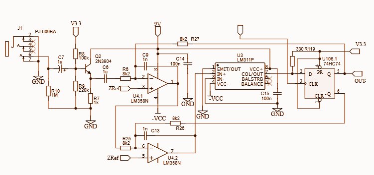
After some component search, I tried to improve the comparator speed by using LM311P instead of LM393. The power supply circuit was also been improved by providing negative voltage -VCC, generated by the charge pump circuit that employs the unused inverter gate of 74HC14. The dual slope single op-amp is also replaced by standard two-stages of single slope integrators. The circuit then looks like in the Figure 4.
Here some detail after modifying the comparator and the supply parts:
- The data output frequency increases to around 110 kHz
- The noise is smooth white noise, which is expected, but the noise level is very strong and unacceptable
- The guitar signal is not much distorted at low level, and high distortion at high level.
- There are very annoying audible aliasing noise, especially on high note strings (G, B, E strings).
- Changing the value of C9 and C13 didn’t affect the data output frequency, indicating that the op-amps of the integrator and or the comparator has been put in the speed-limited operation mode
Improving The Integrator Speed
After done with the fastest available low cost comparator, now time to try to improve the integrator speed. The fastest op-amp of low cost options is NE5532 whish has 10 MHz unity gain. Some high speed op-amp with 50 MHz unity gain bandwidth is available as well but the price is ridiculously high. Here are some results:
- The data output frequency increases to around 800 kHz
- The noise floor is smoother and lower in level, but still very audible and unacceptable
- The aliasing noise is still clearly audible on high string notes, and it is unacceptable
- Changing the C9 and C13 values doesn’t affect the data output frequency, but affect the proportion of the background noise, the aliasing noise, and the signal levels.
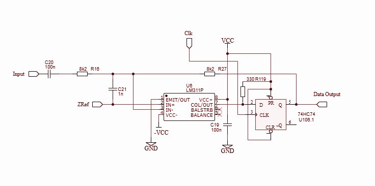
Testing The Comparator’s Speed Limit
After getting desperate with the integrator part that there’s no low cost op-amp with faster performance, then it is also important to see what’s is the fastest possible speed without changing the comparator part. The test is done by removing the active integrator part, replacing the with single stage RC integrator directly from the flip-flop output. Figure 5 shows the tsting circuit.
Here are the result:
- The data output frequency is stuck at around 1.4 MHz, nothing change even if we lower the C21 capacitance.
- The background white noise level is very prominent and unacceptable
- The signal is very stable from low to high level (no added distortion at higher elevel)
- The aliasing noise is almost disappear
The next step, we can test the simplest form of PDM modulator by removing the comparator part, using solely the input threshold of the flip flop to serve as the comparator function. I assume the output frequency would be a perfect half of the clock frequency (at signal level at zero reference), but It’s not tested yet… I will update the result here when I’m done. Thanks for reading, any comments are welcome.