Small Audio Power Amplifier Using 3 Transistors
For some simple applications such as toys, intercom, or small gadgets, there is sometimes a need for small, simple, low cost, or low voltage solution of power amplifier circuit. For this requirement, high fidelity is rarely needed. A modification of amplifier circuit from Bowden’s circuit collection is presented in our article, completed with the guidance on how to modify for other voltage operation.
The Circuit and How It Works
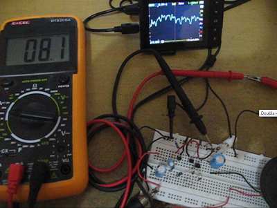
Take a look at the schematic diagram of the circuit shown in Figure 2. It uses only 3 transistors and some passive components. It can drive standard 4-8 ohm loudspeaker. The basic configuration of the amplifier is a push-pull circuit. The complement transistor is not used to drive a transformer but to discharge the dc decoupling capacitor to give full wave alternating current to the loudspeaker. Some components from original circuit (Bowden’s collection) are omitted to make simpler circuitry. The original resistors at TR2 and TR3 emitters are removed, and its ok since we limit the idle current small enough to prevent both transistors get shorted (turning on together and short the current path directly from Vcc to ground).
The original resistor at TR1 emitter is also removed since we can make sure the bias current is automatically adjusted to the proper operating point by feedback mechanism of the biasing circuit (R2, R3, R4, and C3).
DC Feedback for Simple Automatic Biasing
To maximize the potential voltage swing of the output, the junction of TR2 and TR3 emitters should be set at half of the supply voltage (1.5V). At this point, this voltage should produce a proper voltage at TR1’s base that cause TR1 begin to active (0.6V). The biasing voltage is the voltage across R4,
VR4 = 1.5V * R4/(R4+R3+R2)
VR4 = 1.5V * 6.8/(6.8+47+4.7)
VR4 = 0.63V
The feedback mechanism make the resistors selection is not critical, as long as the current is enough to give proper idle current at the TR1 collector. We can make a simple rule by setting the R2-R3-R4 current (half of supply voltage divided by the total R2+R3+R4 resistance) minimum at ten times of the base current (collector current divided by the transistor gain). Lets check it out with the rule, the collector current (at idle condition) is
Ic = (Vcc – 2*Vdiodes)/2R1
Ic = (3V-2*0.6V )/ 2k
Ic = 0.9 mA
At low current condition, the gain (hFe) of the transistor (TR1) is around 100. So the base current will 0.009 mA, and the ten times is 0.09 mA, so the maximum of total R2-R3-R4 resistance is the half supply voltage divided by this current:
Rmax = 1.5V/0.09mA
Rmax = 16.67k Ohm
This requirement is fulfilled by the selected values, since its total resistance is only 16.2 k ohm.
A filtering capacitor C3 is inserted between R3 and R3 to short the signal. Without this capacitor, the circuit will try to regulated to make sure the output will never swing from the half point even when the input signal is applied. Our experiment show distorted negative cycle when we omit this capacitor.
How Push-Pull Operation Works
To ease the explanation on how this circuit enable TR2 and TR3 transistors work complementary, let’s imagine that TR1 is replace by a variable resistor, let’s call it R1′ since its position is symmetric with the R1. At some point of R1′ value, at 1k ohm, which is the set for idle situation, both transistors TR3 and TR2 will be slightly “on” symmetrically. At this idle point, both transistors are set on symmetric small current conduction by keeping small voltage across base-to-base of two transistors, and this is done by D1 and D2. This small voltage is the sum of two voltage drops of two forward-biased diodes. At positive cycle of the sine input signal, R1′ (TR1’s collector-emitter equivalent resistance) will decrease below 1k ohm, TR3 will be cut-off and TR2 will be activated to serve the output (discharging the C2). At negative cycle of the input waveform, the R1′ will get higher than 1k ohm, TR2 will be cut-off and TR3 will be activated to serve more current for serving the output, charging the C2.
Modifying The Circuit for Higher Voltage Operation
If we want to implement this circuit for higher voltage, remember that the output point, the junction between the complementary transistors emitters should be set at the half of supply voltage, so the bias resistors should be recomputed to find proper values. We can select R1 based on the maximum current of the final transistors ant the transistor gain at that maximum current, but always remember that this circuit is not stable if the final transistor get hot. The base-emitter voltage might drop far below the biasing diodes voltage when the transistors get hot, so short current (directly from Vcc to TR3 to TR2 to ground) can be uncontrollable even at idle (no signal) condition. We can increase the R1 to make sure the transistor is operated far below its maximum current handling.
Adding Gain Control and Stabilizing Final Transistors
We can get better performance if we can negotiate with the components count. Inserting a series resistor between TR1 emitter and ground will lower the overall gain of this amplifier, but remember that the inserted resistor is lower than R1 value. A small 500 ohm trimmer potentiometer can to the job for flexible gain adjustment. Inserting a series resistor between the emitter of the final transistor and the output junction will improve the stability against temperature drift. We can use two 0.5 ohm resistors, one for each transistors.