BSMP-BRD Blackstomp Board Manual
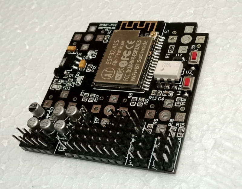
Table of Contents
- I. Schematic Diagram
- II. Bill of Materials
- III. Port Connector Layout
- IV. Potentiometer and Toggle Switch Mounting
- IV.1. Potentiometer Mounting
- IV.2. Toggle Switch Mounting
- IV.3. Reducing Enclosure Mounting Stress
- V. Development-Mode Wiring
- V.1. Wiring Diagram
- V.2. Bill of (Offboard) Materials
- VI. Firmware Programming Through Onboard UART Connector
- VII. Universal Drill Templates
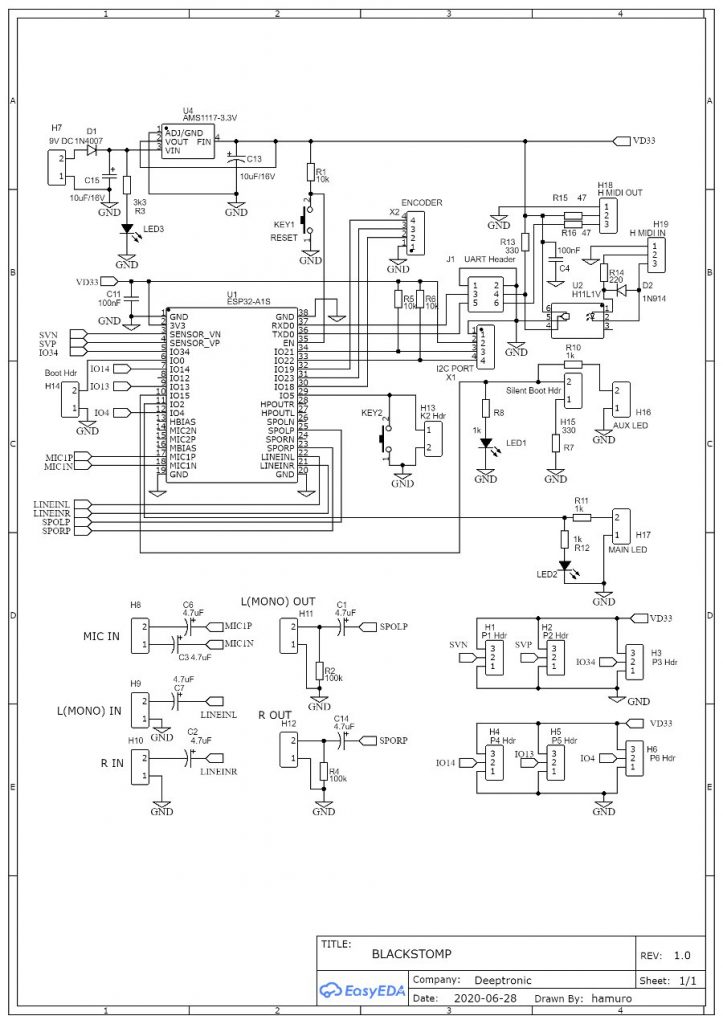
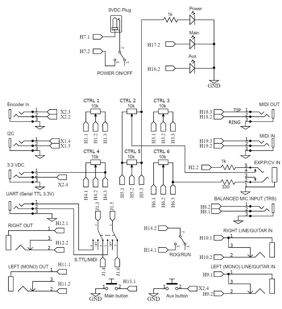
I. Schematic Diagram
II. Bill of Materials
| NUM | NAME | REF | QTY | FOOT PRINT |
| 1 | 100k | R2, R4 | 2 | R0603 |
| 2 | 10k | R1, R5, R6 | 3 | R0603 |
| 3 | 330 | R7, R13 | 2 | R0603 |
| 4 | 1k | R8, R11, R12, R3, R10 | 5 | R0603 |
| 5 | 220 | R14 | 1 | R0603 |
| 6 | 47 | R15, R16 | 2 | R0603 |
| 7 | 10uF/16V TANT | C15, C13 | 2 | CAP-SMD_L3.2-W1.6-R-RD |
| 8 | 4.7uF/16V ELCAP | C14, C1, C6, C7, C2, C3 | 6 | CAP-ELCAP D4MM |
| 9 | 100nF MLCC | C11, C4 | 2 | C0603 |
| 10 | 1N4007 | D1 | 1 | D1206 |
| 11 | 1N4148 | D2 | 1 | SOD-123_L2.8-W1.8-LS3.7-RD |
| 12 | RED LED | LED1, LED2, LED3 | 3 | LED0805 |
| 13 | H11L1V | U2 | 1 | SMD-6_L8.6-W6.4-P2.54-LS9.4-BL |
| 14 | SMD Tactile Switch | KEY1, KEY2 | 2 | KEY-3.0*4.0 |
| 15 | AMS1117-3.3V | U4 | 1 | SOT-223-3_L6.5-W3.4-P2.30-LS7.0-BR |
| 16 | Male Header 1×2 | H7-H17 | 11 | 1×2 P2.54MM |
| 17 | Male Header 2×3 | J1 | 1 | 2×3 P2.54MM |
| 18 | Male Header 1×8 | H20 | 1 | 1×8 P2.54MM |
| 19 | Male Header 1×4 | X1,X2 | 2 | 1×4 P2.54MM |
| 20 | Male Header 1×3 | H1, H2, H3, H44, H5, H6, H18, H19 | 8 | 1×3 P2.54MM |
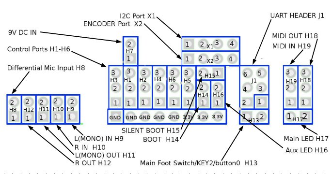
III. Port Connector Layout
IV. Potentiometer and Toggle Switch Mounting
Based on the standard schematic diagram of Blackstomp’s circuit, potentiometer, switch or any other component connected to the control ports is considered as offboard parts. With BSMP PCB, onboard component pads are provided for potentiometers and SPDT toggle switches on H1, H3, H4, H5, and or H6 ports. The PCB-mounted parts could be then securely mounted to the enclosure, holding the board securely inside.
IV.1. Potentiometer Mounting
A right-angle PCB mount potentiometers can be mounted to any of control port pads (H1, H3, H4, H5, and H6) on the bottom side of the PCB, as shown in the Figure 3.
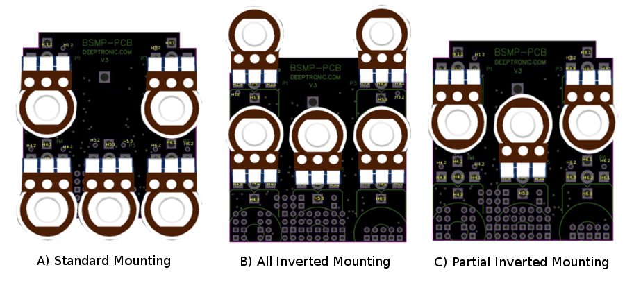
The standard mounting is shown in the Figure 3.A, where the turning direction is clockwise (from minimum to maximum control value). By rotating all of the potentiometers, we can get the inverted mounting like shown in the Figure 3.B. With this configuration, we have to set the inverted flag to “true” in the software to get the normal clockwise direction (from minimum to maximum).
IV.2. Toggle Switch Mounting
Any control port mounting pads can be installed with SPDT toggle switches, like shown in the Figure 4.
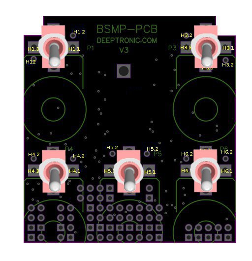
- There are two types of SPDT toggle switches: ON-ON and ON-OFF-ON. The first one provides a 2-position control, and the second provides 3-position control.
- If the type is ON-OFF-ON switch (3-position), then we have to install two small resistors (2x 10k 0.25W) that connect each of the outer leads to the center lead of the switch.
- Use the small rounded pads (next to the bigger square pad) to connect the resistors. For example, if H1 is used for an ON-OFF-ON switch, then install a 10k resistor across H1.2-H1.1 and a 10k resistor across H1.2-H1.3.
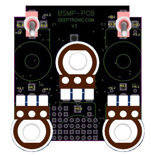
Please note that you can mix toggle switches and potentiometers on one board (see Figure 5 for example) since each control ports has independent configuration in the software. In addition to rotating the potentiometer on the board, you can also find many knob layout configurations by rotating the board itself inside the enclosure.
IV.3. Reducing Enclosure Mounting Stress
When the PCB-mounted potentiometers and switches are secured to the enclosure, it might bend the PCB and introduces some mechanical stress on the soldered SMD components. This stress might cause a microfracture on some components, tracks, or solder joints. The could produce a circuit failure which can be hard to troubleshoot. To reduce the risk of this mounting stress, you can follow the following steps when soldering and mounting the potentiometer and switches:
- Make sure all of the onboard components is fully assembled, including the header connectors.
- Install all the potentiometer and switches to the enclosure, all with loosely installed nut and washer.
- Mount the board to the enclosure-mounted potentiometers and switches by matching all the leads to their respective holes of the soldering pads.
- Align the board in respect to potentiometers, switches, and the enclosures
- Tighten the nuts of all potentiometers and switches while keeping the board aligned without any stress.
- Solder all the leads of the potentiometers and switches.
- Now you can uninstall or reinstall the board by unmounting or mounting the potentiometers and switches to the enclosure with minimal mechanical stress on the board.
V. Development-Mode Pedal Wiring
V.1. Wiring Diagram
The recommended wiring diagram for development-mode is shown in the Figure 6. The wiring is the same with the Blackstomp’s recommended development-mode pedal wiring.
V.2. Bill of (Offboard) Materials
| NUM | PART NAME | QTY. | Connection Reference | Connection Description |
| 1 | DC socket for 9V DC input. | 1 | H7.1 | DC input |
| 2 | SPST (normally open, momentary) foot switch | 2 | H13.2, X2.4 | Main and aux button |
| 3 | Red LED | 3 | R(1K), H16.2, H17.2, | Power, main, and aux LED indicators. |
| 4 | 1K Resistor | 2 | VD33, H2.2 | Power LED and control port current limiter |
| 5 | 330R Resistor | 1 | VD33/H6.3 | EXP.P/CV 3.3V source current limitter |
| 6 | SPDT ON-ON toggle switch | 2 | H14, H7.2 | PROG/RUN switch and ON/OFF switch |
| 7 | DPDT ON-OFF-ON toggle switch | 1 | J1 | UART/MIDI switcher. |
| 8 | TS socket 6.3 mm | 4 | H9, H10, H11, H12 | L/R inputs and outputs |
| 9 | TRS socket 6.3 mm | 1 | R(1K), R(330), POT | EXP.P/CV IN. |
| 10 | TRS socket 3.5 mm | 7 | H8, H18, H19, J1, X1, VD33, X2 | MIC, MIDI, UART, I2C, DC OUT, ENC. IN |
| 11 | Potentiometer B10K | 6 | H1, H2, H3, H4, H5, H6 | Control Knobs |
Please note that the potentiometers, although it can be PCB-mounted on BSMP-PCB, are considered as offboard parts because the standard Blackstomp circuit doesn’t specify potentiometer as the connected control part. Other important thing to note is that we still need many wires with female Dupont connector to connect the offboard parts to the onboard header connectors.
VI. Firmware Programming Through Onboard UART Connector
BSMP-BRD Blackstomp board comes with unprogrammed security bits (the secure boot and flash encryption bits), so it can be programmed and reprogrammed using UART jumper header J1 before putting it into the pedal enclosure. This is useful for production, not for development-mode pedal, since (ideally) the final product shouldn’t be equipped with the UART/Serial TTL programming port. With all the on-board parts have been assembled, we can now program the firmware through the UART port:
- Run your ESP32 flash uploader/programmer application (the Arduino IDE or ESP-IDF tools) on your PC/laptop, and connect the application to USB-to-TTL cable/converter.
- Power the board by connecting a 9V DC power supply to the H7 header connector, make sure the onboard power indicator (LED3) works.
- Connect the J1.1 (GND), J1.3(RX), and J1.5(TX) to the USB-to-TTL cable at GND, TX, and RX
- Insert a jumper to boot header H14 to ground the IO0 port of the ESP32-A1S module.
- Press the onboard reset button KEY1, now the board will wait for firmware data transfer on the UART.
- Execute the upload menu in the flash uploader/programmer application in your PC/laptop. Wait until it done.
- To start running the uploaded firmware, pull out the jumper form boot header H14 and press the onboard reset button KEY1.
- To reprogram or reupload a new firmware, go to step 4.
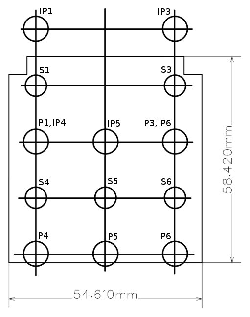
VII. Universal Drill Templates
Because BSMP PCB is not designed for just one effect type, a universal drill template shown in the Figure 7 can be used to make various knob and switch configuration.
- The hole’s diameter is 7 mm for potentiometers and 6 mm for toggle switch.
- The holes P1, P3, P4, P5, and P6 are the holes for installing potentiometers mounted on H1, H3, H4, H5, and H6.
- The holes IP1, IP3, IP4, IP5, and IP6 are the holes for installing inverted (rotated) potentiometers mounted on H1, H3, H4, H5, and H6.
- The holes S1, S3, S4, S5, and S6 are the holes for installing toggle switches mounted on H1, H3, H4, H5, and H6.
- Make sure the size of board outline is 58.42 mm x 54.61 mm on the actual printed template.