BSCORE DEV PEDAL PCB BUILD DOCUMENT
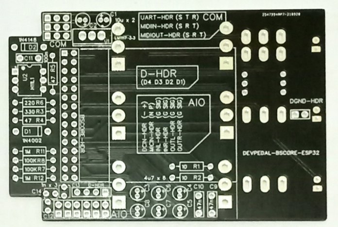
Table of Contents
- Schematic Diagram
- Off-Board Parts Wiring Diagram
- Top Layer Layout
- Bottom Layer Layout
- On-Board Part List
- Off-Board Part List
- Printable Enclosure Drill Template
- Printable Enclosure Label
- Building Guide
Contents
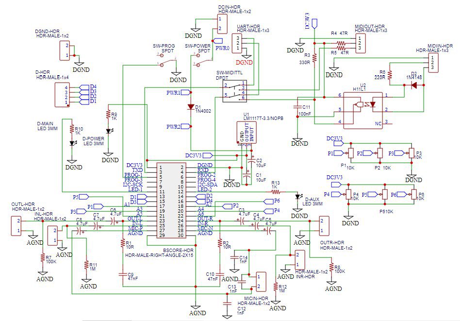
1. Schematic Diagram
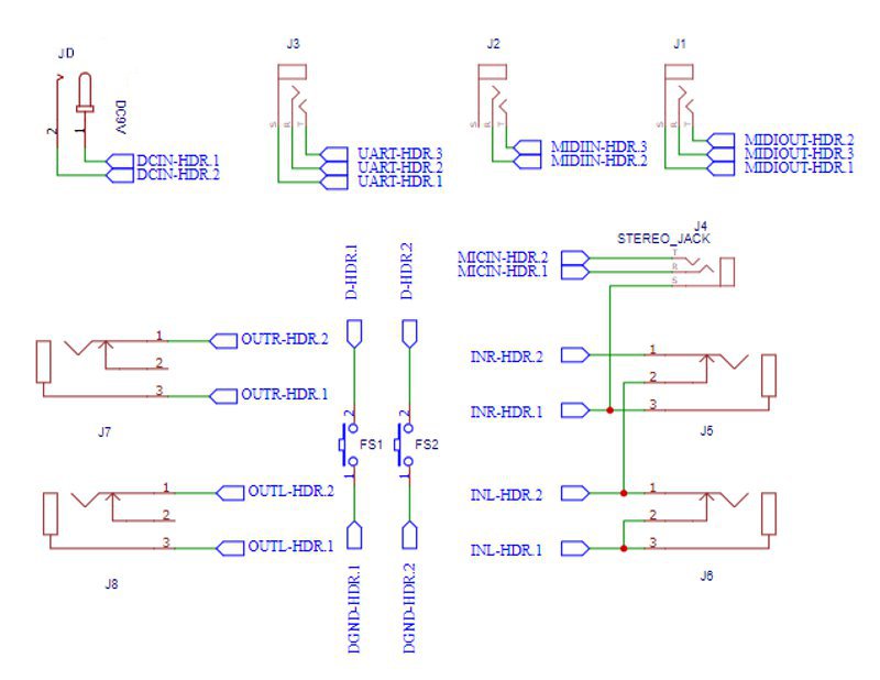
2. Off-Board Parts Wiring Diagram
3. On-Board Part List
Note: C11 uses multi-layer ceramic capacitor (MLCC) because it should have maximum height of about 5 mm when soldered onto the board, you can use value between 0.1 to 1uF for this capacitor.
| ID — | NAME | DESIGNATOR | QTY |
| 1 | BSCORE Module + MALE-HEADER RIGHT-ANGLE-2X15 | BSCORE-HDR | 1 |
| 2 | 10uF/16V electrolytic capacitor | C1,C2 | 2 |
| 3 | 4.7uF/16V electrolytic capacitor | C3,C4,C5,C6,C7,C8 | 6 |
| 4 | 47nF Capacitor | C9,C10 | 2 |
| 5 | 100nF Multilayer Ceramic | C11 | 1 |
| 6 | 1nF Capacitor | C12,C13,C14 | 3 |
| 7 | 1N4002/1N4001/1N4007 Diode | D1 | 1 |
| 8 | 1N4148 Diode | D2 | 1 |
| 9 | LED 3MM (RED) | D-AUX,D-MAIN,D-POWER | 3 |
| 10 | MALE HEADER-1×4 | D-HDR | 1 |
| 11 | MALE HEADER-1×2 | DCIN-HDR,DGND-HDR,INL-HDR,INR-HDR,MICIN-HDR,OUTL-HDR,OUTR-HDR | 7 |
| 12 | MALE HEADER 1×3 | MIDIIN-HDR,MIDIOUT-HDR,UART-HDR | 3 |
| 13 | B10K, right angle PCB-Mount potentiometer | P1,P2,P3,P4,P5,P6 | 6 |
| 14 | 10R , 0.25W Resistor | R1,R2 | 2 |
| 15 | 330R , 0.25W Resistor | R3 | 1 |
| 16 | 47R , 0.25W Resistor | R4,R5 | 2 |
| 17 | 220R , 0.25W Resistor | R6 | 1 |
| 18 | 100K, 0.25W Resistor | R7,R8 | 2 |
| 29 | 1K , 0.25W Resistor | R9,R10,R13 | 3 |
| 20 | 1M , 0.25W Resistor | R11,R12 | 2 |
| 21 | DPDT ON-OFF-ON Toggle Switch | SW-MIDITTL | 1 |
| 22 | SPDT ON-ON Toggle Switch | SW-POWER,SW-PROG | 2 |
| 23 | LM1117T-3.3 Voltage regulator IC | U1 | 1 |
| 24 | H11L1 optocoupler | U2 | 1 |
4. Off-Board Part List
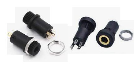
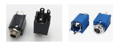
Note: Use isolated 3.5 mm TRS sockets for J1-J4 (like shown in the Figure 4), since the board has separate audio ground and digital ground to minimize the digital noise. For audio input-output (J5-J8), use mono or stereo socket with small case overhead (like shown in the Figure 5), so it could fit in this critical spacing design.
| ID — | NAME | DESIGNATOR | QTY |
| 1 | SPST Momentary Footswitch | FS1,FS2 | 2 |
| 2 | ISOLATED 3.5 mm TRS socket | J1,J2,J3,J4 | 4 |
| 4 | MONO audio socket 6.35 mm | J5,J6,J7,J8 | 4 |
| 5 | ISOLATED 2.1 mm DC socket | JD | 1 |
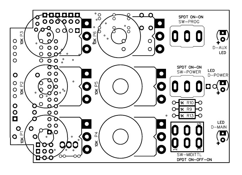
5. Top Layer Layout
6. Bottom Layer Layout
7. Printable Enclosure Drill Template
Download in PDF document (right-click and save)
8. Printable Enclosure Label
Download in PDF document (right-click and save)
9. Building Guide
- Make sure the enclosure has been drilled, painted, and labeled.
- Solder all components of the top layer, including all the header connectors. Make sure the LM1117-3.3V is mounted on the board to have as short as possible height.
- Solder all bottom layer resistors (R9, R10, R13), those are all bottom layer components except the potentiometers, LEDs, and switches.
- To reduce the mechanical stress on the PCB when mounted the the enclosure through by potentiometers and switches, follow these steps:
- Install all potentiometers (P1-P6) and toggle switches (SW-POWER, SW-MIDITTL, SW-PROG) loosely to the enclosure.
- Mount the PCB to the mounted potentiometers and switches and align perfectly with the enclosure, keep it aligned without soldering.
- Tighten the nuts of all the potentiometers and switches while keeping the board mounting aligned, still without soldering.
- Solder all potentiometers and switches except P1, P2, and P3.
- Cut the leads of P1, P2, and P3 as short as possible, so they have zero height before get soldered.
- Solder P1, P2, and P3 without excessive tin so it produces thin or flat soldering surface in the top layer. This will make the BSCORE module insertion possible/easier.
- Unmount the board and the potentiometers assembly from the enclosure.
- Re-solder the potentiometers P1, P2, P3 from the bottom to add more strength, but be careful not to let the tin flows to the other side.
- Mount the LEDs with the following steps:
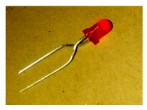
- Twist the LEDs for D-POWER, D-AUX, and D-MAIN 90 degrees before mounting them to the PCB, as shown in the figure 8. This twisting enables omni-directional horizontal adjustment after get soldered to PCB.
- Mount each LEDs and adjust the height to get aligned with the adjacent switch as the reference.
- Solder the LEDs from both sides (top and bottom layer) to get maximum strength against pushing and pulling off the board.
- Cut all the excessive components leads.
- Re-mount the board assembly to the enclosure through the potentiometers switches, secure their nuts tightly.
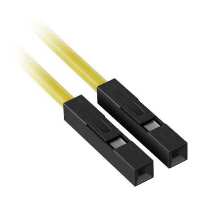
- Mount the footswitches (FS1, FS2) to the enclosure, and wire them to the board using single female header cable jumper (Figure 9). See Figure 3 as the wiring reference for off-board parts.
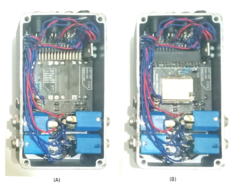
- After the footswitches get wired, you can mount all other sockets (JD, J1-J8) to the enclosure and wire them to the board using cable jumper/single female header in any order (Figure 10(A)). See Figure 3 as the wiring reference for off-board parts.
- Insert the BSCORE Module to its header (Figure 10(B)).
- Secure the enclosure with its base-lid, now the pedal is ready to use (Figure 11).