Envelope Detector Circuit with Separate Attack/Rise and Decay/Release Time Settings
Introduction to Envelope Detector Circuit
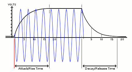
Envelope detector circuit is used to get the amplitude profile of a signal. Some important properties of an envelope detector are attack or rise time and decay or release time. In the Figure 1, a signal is plotted in blue, and the detected envelope is plotted in black. Since it employs capacitor for filtering inside the detection process, the process of charging and discharging of the the capacitor produces the attack and decay phenomenons. In some audio processing processes, such signal compressor or automatic wah effect, the characteristic of attack/rise time and decay/release time might produce some benefits and need to be controlled to produce various unique results.
Simple Envelope Detector Circuits
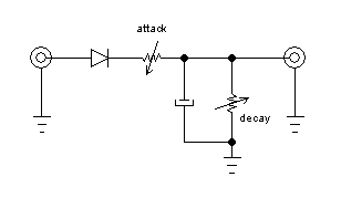
A very simple passive envelope detector circuit’s schematic diagram is shown in the figure 2. The detector assume a very low impedance in the input source and a very high impedance in the output devices. The drawback of this circuit is that the gain of the detector is affected by decay and delay setting, means that increasing attack time and or decreasing decay time will reduce the envelope gain. This would be difficult and inconvenient in many applications.
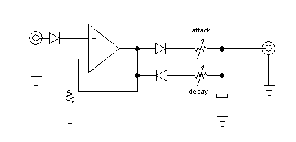
One improvement can be made using op-amp as an active amplifier. As seen in the figure 3, now the setting of the attack/rise time and decay/release time has separate paths through different orientation diodes. The drawback of this circuit is that the diode adds a dead-zone, when the difference between the output voltage (capacitor’s voltage) and the output of the op-amp falls within bias range of the diode. For silicon diode like 1N4148, both diode will be inoperative if the voltage difference s less than 0,6 volts.
The Ultimate Improvement: Separate Active Attack-Decay Rectification
To eliminate the bias error comes from the diodes, I have designed an envelope detector with separate attack and decay active rectification.
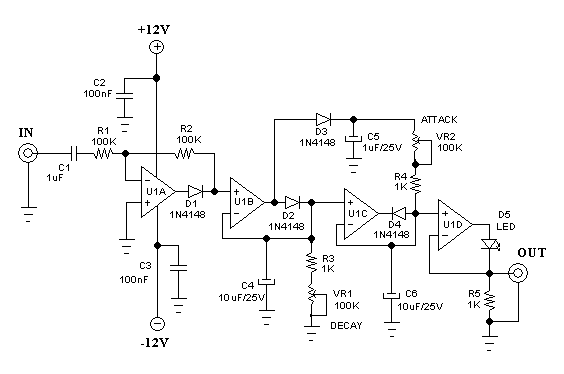
Operational amplifier (op-amp) U1A provide full-wave rectification, op-amp U1B provides active decay rectification, and op-amp U1C provides active attack rectification. At U1B, if the input is higher than the output then the output will be corrected as fast as possible since the op-amp will be actively drive the diode D2. But when the input gets lower than the output, the output will be slowly decayed through the resistor R3 and VR1 since the diode disconnect it from the strong negative pulling of the op-amp output. At U1C op-amp, the diode is reversed, so the op-amp will act to discharge as fast as possible whenever the input is lower than the output by actively driving the diode. But when the input is higher than the output, the capacitor will be charged slowly through the R4 and VR2. Ideally, VR2 should be connected to the buffered signal from D2 output, but it will need one additional op-amp. To avoid adding an additional op-amp while approximating D2 output, a diode D3 and a C5 capacitor is added to provide fast attack signal without affecting the decaying process of C4 capacitor discharging. Op amp U1D is provided to buffer the output, and D5 LED is provided as an indicator. If the indicator is not needed then D5 can be shorted directly to the output and the feedback path, and R5 can be omitted. See the circuit in action in the following video.
The background description is well presented. I simulated this circuit, and it works perfectly. I adjusted a few component values (C6 was a bit too high for my application). The Hamuro generator name will be used to describe this circuit in my compressor. Thank you for this Hamuro, it’s a very good technical solution.
You are welcome, it is more than happy to find my circuit design useful for others.
I’m going to give this a whirl in one of my designs. Its a modification to a Dunlop GCB95 Wah, the plan is to add an envelope filter (Auto wah) mode. My previous attempt was an op amp precision rectifier circuit with filtering and it worked well but my attempt at adding adjustments didn’t do much. Normally I would persevere and eventually get what I’m after but I have far too much on the backburner so thanks for sharing your design.
Thanks for posting this Hamuro. This looks like a circuit that I need! Can you tell me what the output voltage swing is? Is it 12v to 0v or 12 to -12V? I need something like this to drive logic – perhaps an addition of a open collector transistor?
Because of the D5 LED and the op-amp’s output swing limitation, the output will swing from 0v to about 8V. You have to discard the D5 to give about 0-10V swing.
Great Hamuro, thanks for sharing. Unfortunately a long DECAY time also affects (enlarges) the attack time with the valued you are giving.
Still looking for another solution…
Regards from germany
Michael
Ah, another comment: D1 is absolutely unnessesary in the circuit….
Without D1, it becomes an inverting amplifier, not a full wave rectifier. At the positive cycle of the input, the input of the second op amp should detect a positive voltage exactly at the same level with the input, not the inversion of the input. It won’t happen without D1.
Very cool.
Somehow I don’t really get it to work.
My output is always inverted
In passive scheme there are atack and decay. What if I need realize is any possibility to make it?