CD4093 Switch-Mode Current Limiter for LED Driver
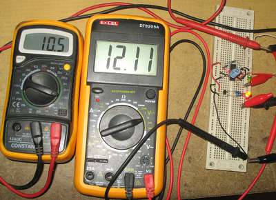
Figure 1. Assembled Switching Current Limiter LED Driver Circuit
A LED driver provides power regulation so the working voltage and current applied to a LED is kept stable while maintaining high efficiency in various supply voltage condition. Using a Schmidt-trigger NAND gate, we can design a LED driver with switching technology. Switching technology is developed to minimize power loss power control. The idea of this technique is by fully switching-on and switching-off a solid-state device, so the dissipated power by this device is neglected.
The Circuit, Schematic Diagram, and How It Works
The core component of this circuit is CD4093 NAND gate, which has Schmidt-trigger input mode, as shown in the schematic diagram (Figure 2). Trigger input mode allow the circuit to oscillate in a clearly-defined period. Let’s assume the output is off at the first time of powering the circuit, so no current flow at LED and R3, so no current flow in R2 to bias the base-emitter and the transistor is off. Because the transistor is inactive then the collector-emitter is open (disconnected), so the pin 1 and 2 of UA gate goes high and activate the gate (in 3 goes to low). This activation will deactivate the gate UB, UC, and UD (their pins go high), so now the current will flow through the inductor L1, this current will increase until the voltage at R3 reach the TR1 activation voltage, the bias point of base-emitter voltage, which is around 0,6V. By selecting R3 as 56 ohm, then the current level that will activate the transistor is around 10 mA. After the transistor activation, the system will be turned-off and the current will decrease until the transistor is deactivated again.
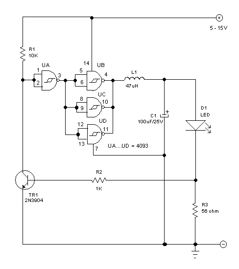
Figure 2. The Schematic Diagram of CD4093 Switching LED Driver Circuit
The gate UB, UC, and UD are paralleled to give stronger current, and 10 mA is the safe point according to specification the typical current handling of each gate’s output. We cans still safely increase the R3, but don’t decrease it to keep the average current below 10 mA. The input voltage range of CMOS series cover the 5-15V spec of this circuit, which is suitable for automotive environment. If needed, the pin 2 of the IC can be disconnected from its connection and can be controlled independently by connecting to ground (0V) to turn-off the circuit, or connecting to Vcc to turn-on the circuit. The video at our Youtube channel below shows the stability of the current (as shown in the first meter), regardless of the changing input voltage (shown in the second meter).