Full-Adder Circuit, The Schematic Diagram and How It Works
Introduction
Full-adder circuit is one of the main element of arithmetic logic unit. It is the full-featured 1-bit (binary-digit) addition machine that can be assembled to construct a multi-bit adder machine. We can say it as a full-featured addition machine since it has “carry input” and a “carry-output”, in addition to the two 1-bit data inputs and one 1-bit data output. Before presenting the hardware circuit for the full-adder, the basic of binary addition concept will be presented first in this article for better understanding.
Binary Addition Concept: Using “Carry” for Multi-Digit Operation
In order to design a digital (binary) adder machine, binary number addition process can be analyzed as digit-by-digit operation. So, the whole operation can be broken down into simple logical operation steps. By getting the simple logical operation, then a functional machine can be easily implemented using logic gates circuit. Now take a look at the Figure 1 for example.
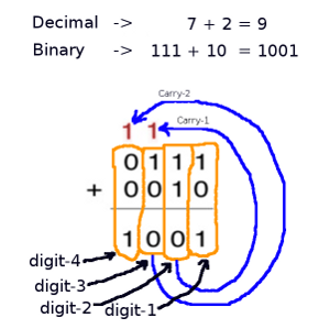
To add two binary numbers 111 (7 in decimal) and 10 (3 in decimal), first we add the digit-1 (the least significant bit). The operation on the input show the operation of 1 + 0, and the result is 1, and it fits in one digit place so there no “carry” of the digit-1 operation. The next step is operating the digit-2 addition, and it shows 1+1. The result of this addition should be 10, but we have to place the least significan digit (0) in one digit of the result (the digit-2), so the most significant bit of the result (1) will be separated as the “carry” output of the digit-2 operation, designated as carry-1 in the picture. The next operation, the digit-2 operation will be similar with the digit-2 operation but the result of the addition is added by carry-output of the previous digit operation before placing the result in the corresponding digit position. As we can see, every digit operation (except for the least significant bit) is made by adding the bit-data input, then add the carry-data from the previous digit operation, and passing the carry-output (if any) to the next digit operation.
Half-Adder Circuit
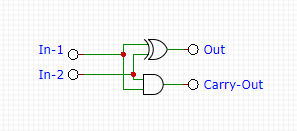
In the previous example, the first operation is adding two 1-bit data of the least significant bits of two binary numbers. This operation needs a circuit with 2 inputs (the least significant bit of the first operand and the least significant bit of the second operand). We also need two outputs from this circuit, 1-bit for the data-output and 1-bit for the carry-output. Now such circuit is called a half-adder circuit. It is basically a 1-bit binary adder with 2-bit output. The schematic diagram of the circuit is shown in the Figure 2.
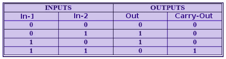
The operation of this half-adder circuit can be described by the following truth table (Figure 3), which show all possible combination of the input and the output’s response of the circuit.
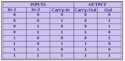
Full-Adder Circuit
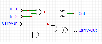
To process the addition of digit-2 or the higher digits in binary addition, one additional input, the carry-input is needed to process the carry-output from previous digit 1-bit addition. Therefore, we need more complex circuit that has 3 inputs and two outputs. A circuit that has similar function with half-adder but with additional carry-input, and such circuit is called a full-adder circuit. Here is the schematic diagram of the circuit (Figure 4)
To describe the operation of the circuit, a truth table of full-adder circuit is shown in the Figure 5. It shows all possible combination of the 3 inputs (In-1, In-2, Carry-In) and it’s outputs response (Out, Carry-Out).
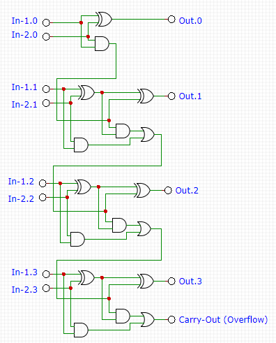
Multi-Digit Adder Circuit
After looking at the binary addition process, half-adder circuit, and full-adder circuit, now we can build a multi-digit binary adder by combining the half adder and full adder circuit. For example, if we want to implement a 4-bit adder circuit, we can combine 1 half-adder and 3 full-adder. The first half-adder has no carry input since it is the first digit operation that accept no carry from non-existent previous digit operation. The carry-output of the first half-adder circuit is fed into the carry-input of the second adder circuit (the first full-adder circuit). The point is that the carry-output of one stage is fed to the carry-input of the next stage, so we can construct any multi-bit wide binary adder. The schematic diagram of a 4-bit adder circuit is shown in the Figure 6.
The carry-output of the 4-bit adder circuit can be viewed as overflow flag, or just simply as the 5th bit of the result register. When we use it for arithmetic logic unit (ALU), we can also use full-adder circuit for all unit for more programmable features. By doing this, we can implement more bit processing by operating the addition per 4-bits (per nibble), and we can just set the carry-input as 0 for the least significant nibble.